Project COFISIS (2008-2012)
"Fabrication of low-cost superlattices for the thermal management of electronic systems"
Grant : ANR-07-PNANO-047
 Project Goals
 Organisation
Work at ESIEE Paris
Publications
Project Goals
The objective of the project COFISIS was to fabricate low cost metamaterials in order to increase their effective thermal conductivity and hence increase their thermoelecric factor of merit. Final applications are 1) the temperature reduction of localized hot spots in electronic systems and integrated circuits, with acceptable manufacturing costs, 2) the recovering of the thermal energy "wasted" by the components to reduce the consumption of energy by the electronic systems.Metamaterials offer the benefit of obtaining improved physical properties over natural materials. In this work, we explored a new variety of thermoelectric metamaterials based on silicon micro- and nano- structuration, in the form of vertical superlattices for use in energy-related applications. Additionally, we focused on a route towards fabricating these materials using simple and low-cost means compared to prior attempts.
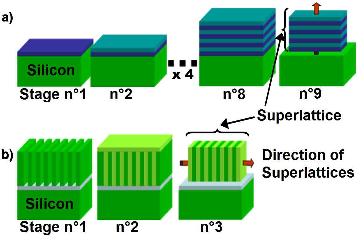
Principle of vertical supperlattices in silicon. a) traditional planar approach, b) COFISIS approach
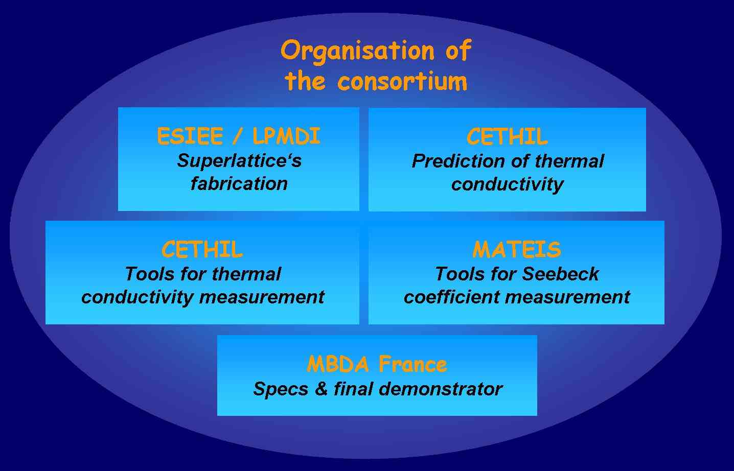
Organisation of the consortium
Work @ ESIEE Paris
At ESIEE Paris, we used both top-down and bottom-up approaches towards fabricating vertical nanoscale structures from single-crystalline silicon. A novel proposed vertical architecture raised technological challenges that were tackled through the exploration of original experimental techniques for producing high aspect ratio (HAR) structures in an effective manner and over large surface areas. These techniques include the use of traditional lithography patterning and subsequent extrusion of volumic structures. Additionally, the use of nanofibers and diblock copolymers as templates for further etching of HAR silicon nanostructures were tested to bring us closer to the ultimate goal of the project.Very high aspect-ratio in silicon using Deep Reactive Etching
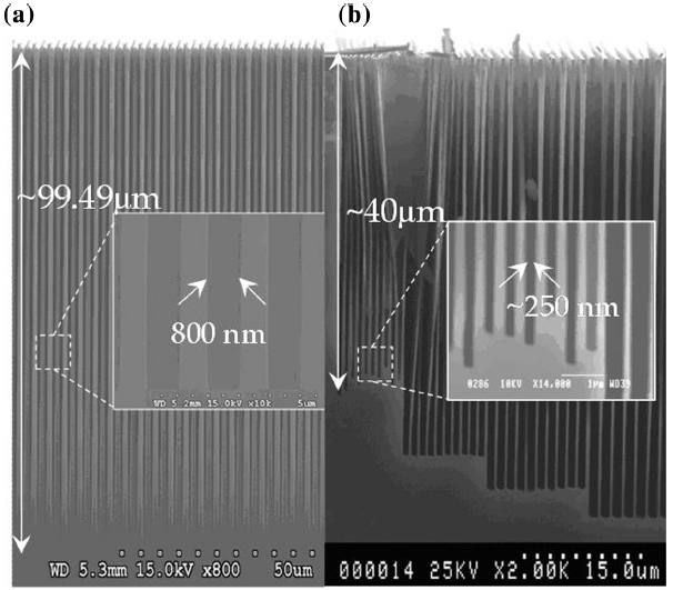
High aspect ratio (HAR) structures manufactured using the Bosch process:
(a) 800 nm-wide trenches with a depth of 99.5 lm (aspect ratio 124:1) and
(b) 250 nm-wide trenches with a depth of 40 lm (aspect ratio 160:1).
Some of the walls collapsed during the dicing procedure .
(a) 800 nm-wide trenches with a depth of 99.5 lm (aspect ratio 124:1) and
(b) 250 nm-wide trenches with a depth of 40 lm (aspect ratio 160:1).
Some of the walls collapsed during the dicing procedure .
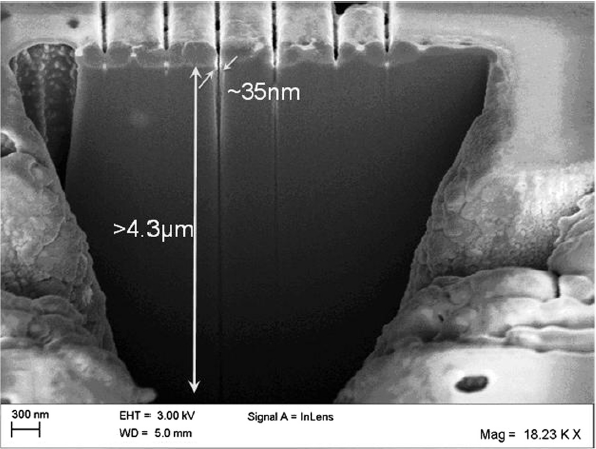
Scanning electron microscope (SEM) image of a 35 nm-wide trench etched to a depth greater than 4.3 µm,
hence with aspect ratio of more than 125:1.
A rectangular hole was etched using the FIB to allow cross-sectional visualization.
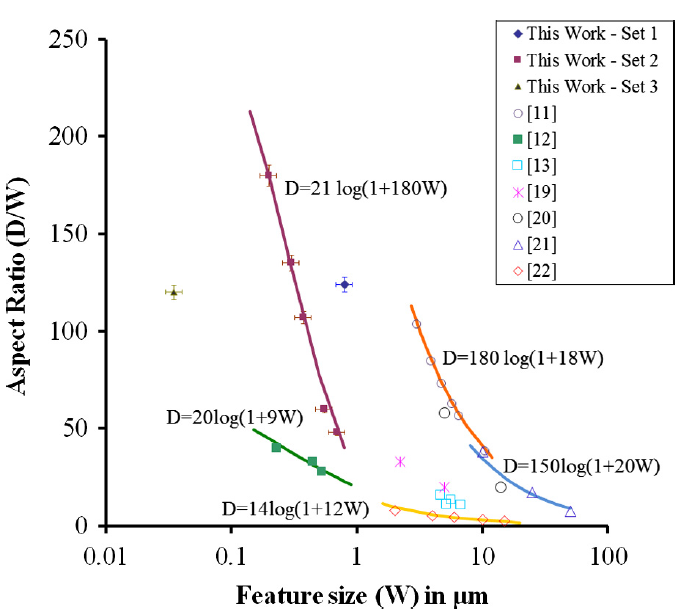
Aspect ratio versus feature size as studied by various groups for feature sizes
ranging from tens of nanometers up to tens of micrometers [1].
hence with aspect ratio of more than 125:1.
A rectangular hole was etched using the FIB to allow cross-sectional visualization.
Aspect ratio versus feature size as studied by various groups for feature sizes
ranging from tens of nanometers up to tens of micrometers [1].
All data are found to fit well with the proposed following two-parameter logarithmic:
AR = [a.log(1+b.W)]/W
where AR is the aspect ratio, W is width of the features (in µm), and a and b
are constants with units of µm and 1/µm,
respectively, that depend on the etching recipe being used. The aspect
ratio is calculated as D/W, where D is the etch depth at the bottom of the trench (see [1] for more details).Related publications
Journals
 “Very High Aspect
Ratio Deep Reactive Ion Etching of Sub-micrometer Trenches in Silicon”, J. Parasuraman, A. Summanwar, F. Marty, P.
Basset, D. E. Angelescu, C. Bunel and T. Bourouina, Microelectronics Engineering, vol. 113, pp. 35-39, Jan.
2014
“Very High Aspect
Ratio Deep Reactive Ion Etching of Sub-micrometer Trenches in Silicon”, J. Parasuraman, A. Summanwar, F. Marty, P.
Basset, D. E. Angelescu, C. Bunel and T. Bourouina, Microelectronics Engineering, vol. 113, pp. 35-39, Jan.
2014
-
“Investigation
of the thermal properties of thin solid materials at different temperature
levels using a set of microresistors”, A. Assy, S. Gomès, P. Chantrenne, N. Pavy, J. Parasuraman, X. Kleber and P. Basset, Microelectronic Journal, 2013
- "Thermal Conductivity and Thermal Boundary Resistance of Nanostructures",
K. Termentzidis, J. Parasuraman, C. Abs Da Cruz, S. Merabia, D.
Angelescu, F. Marty, T. Bourouina, X. Kleber, P. Chantrenne and
Philippe Basset, Nanoscale Research Letters, vol. 6:288, 2011
Conferences
- “New thermal method for the characterization of solid materials at different temperature levels”, Proceeding of the 18th International Workshop on Thermal investigations of ICs and Systems (Therminic’12), A. Assy, S. Gomès, P. Chantrenne, Nicolas Pavy, J. Parasuraman, X. Kleber and P. Basset, Budapest, Hungary, 2012
- "Collective
Fabrication of Inexpensive
Superlatices in Silicon for the thermal management of electronic
systems", P. Basset, P.
Chantrenne and X. Kleber, 4th European
Advanced Technology Workshop On Micropackaging and Thermal
Management,