Tribo-electric/electret (Nano) Generator TENG)
Grants:
CNRS, Campus France
Modeling
Devices
Conditioning circuit with micro-plasma switch
Publications
Modeling
Simple TENG model
In addition to the model proposed by Niu et al, we have
proposed a lumped model directly inspired from the
traditional electret Kinetic Energy Harvester. This model is
suitable for PSpice and can easily take into account practical
specifications of the TENG for accurate conditioning circuit
simulations.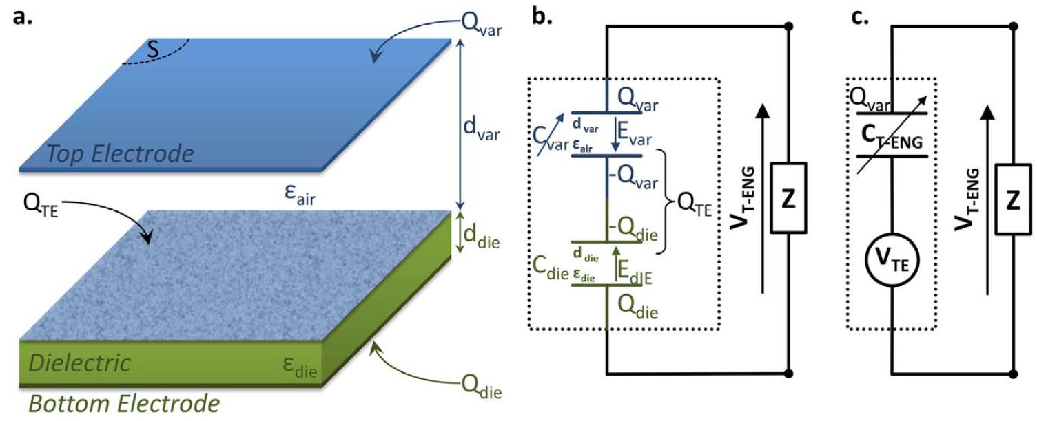
VTE is a constant voltage source representing the charge trapped in the the triboelectret layer. It is independant from the mobile electrode position and from the load. It can be directly measured with an electrostatic contactless volmeter, or, if the layer is not accessible, using an electrical technique we have developped in purpose.
CTENG is the capacitance measured accross the TENG terminals. It can be obtained by measuring the phase shift in an RC circuit.
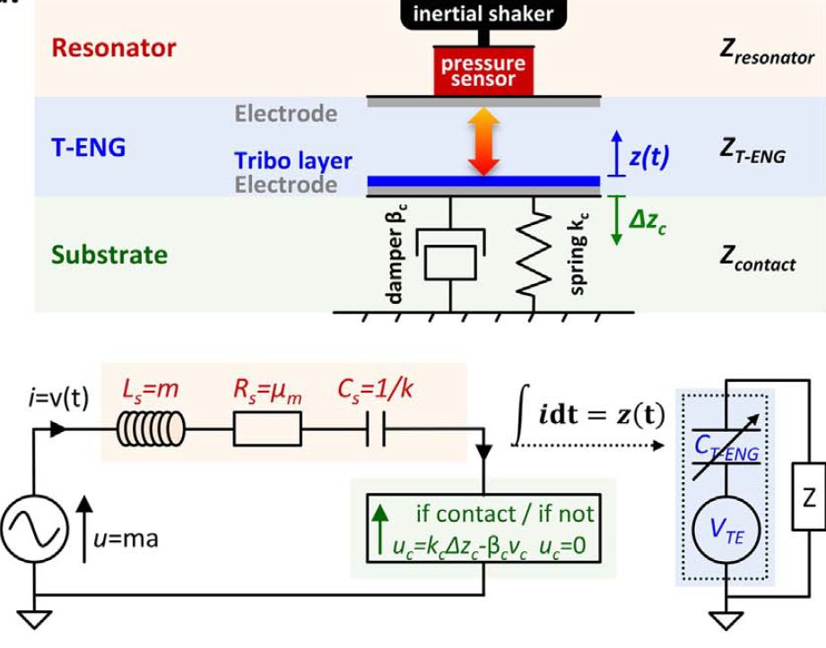
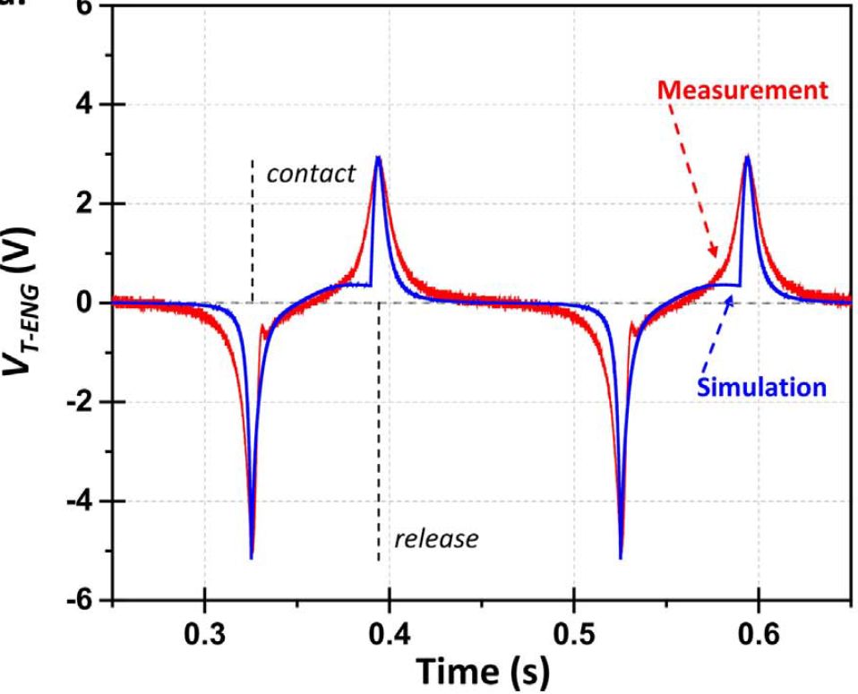
In this work, we have also modelized the effect of the mechanical contact.
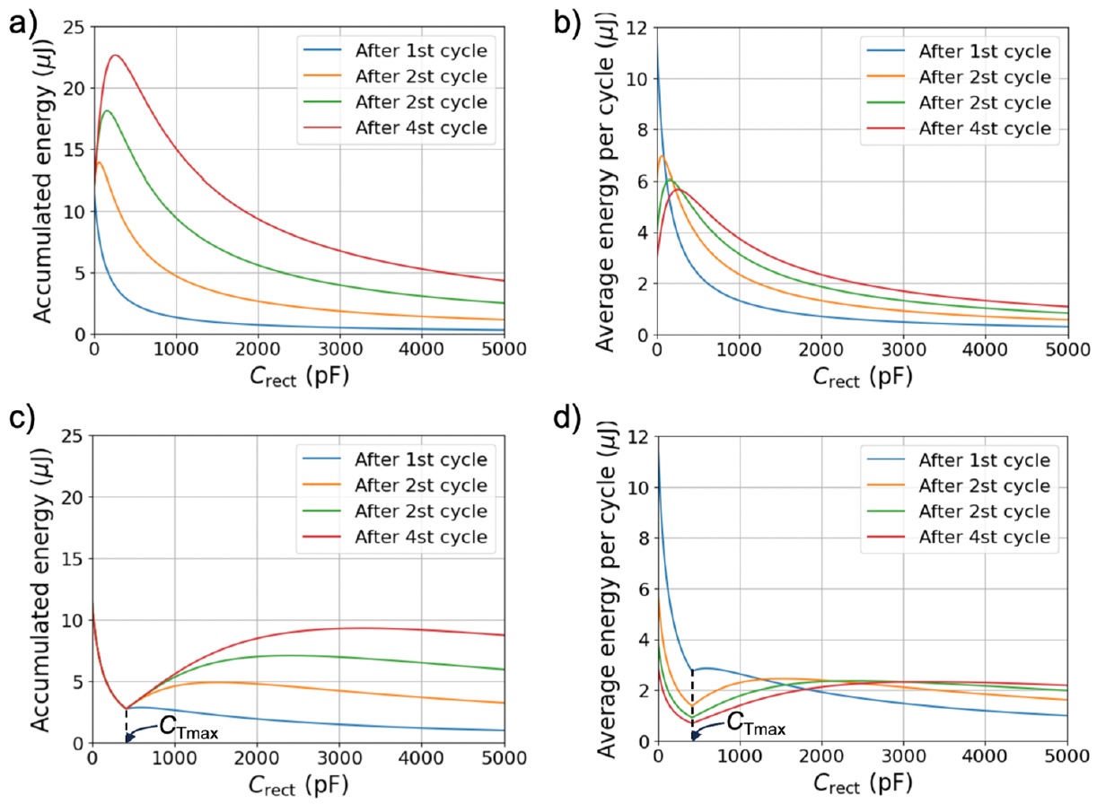
Optimization of a two-stage power management
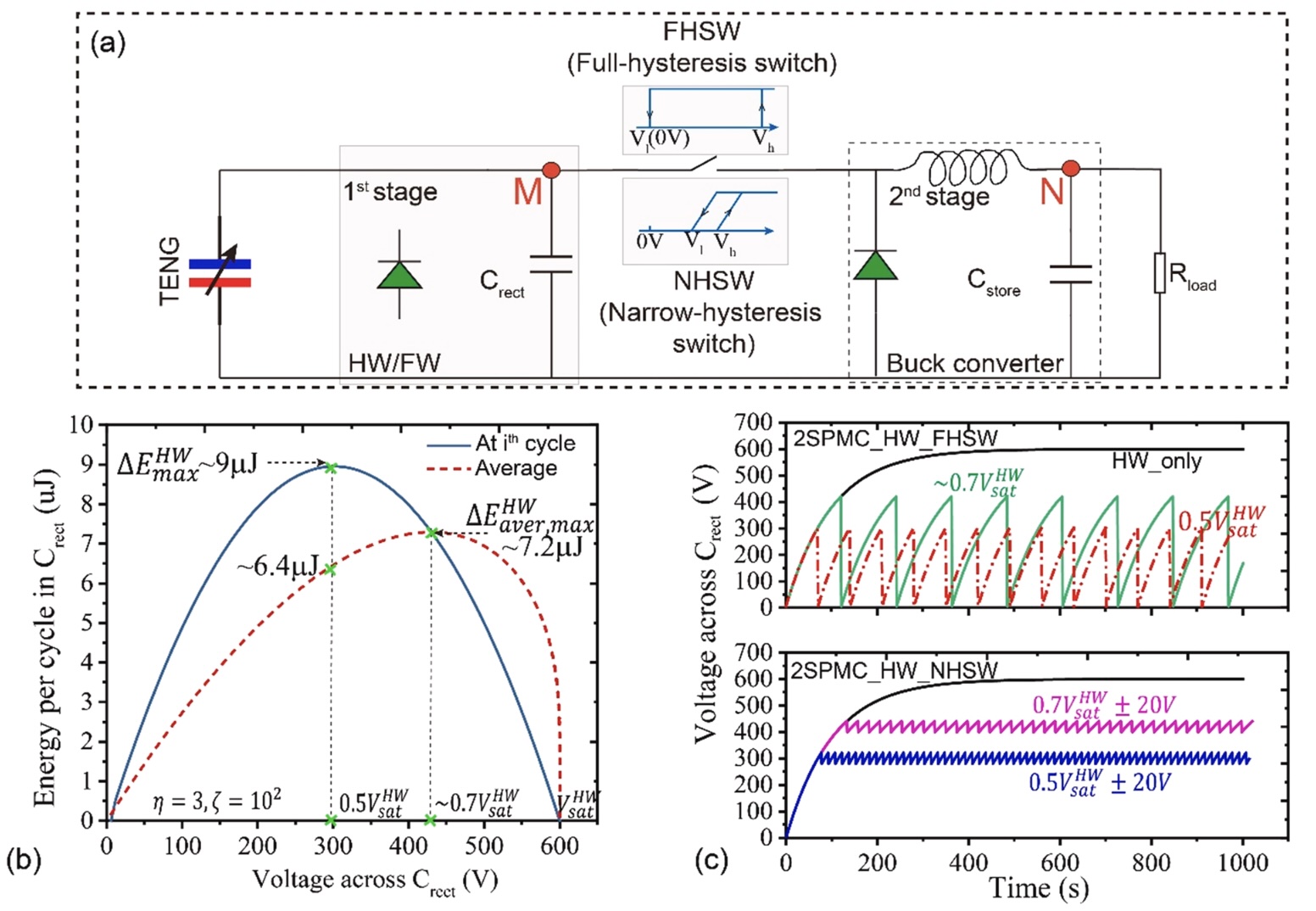
Simulation results of a two-stage power management circuit (2SPMC). (a) Schematic of the 2SPMC. (b) Energy and average energy per cycle in Crect using the HW rectifier. (c) Voltage across Crec with two levels of switch hysteresis.
Optimization for a small number of mechanical actuations
We have presented an optimization framework to maximize
the energy conversion in the early stages of transducer
operation by tuning the output capacitor (Crec) of the DC
rectifier. Through a combination of analytical modeling,
SPICE simulations, and experimental validation using a
custom test bench, we show that after the first mechanical
actuation, tuning Crect to a value close to the minimum
value of the TENG capacitance, and choosing the half-wave
rather than the full-wave rectifier configuration, can
drastically enhance the energy conversion. For the first
actuation, half-wave and full-wave are equivalent as long
as Crect is minimized and less than the maximum value of
the TENG capacitance.
Devices
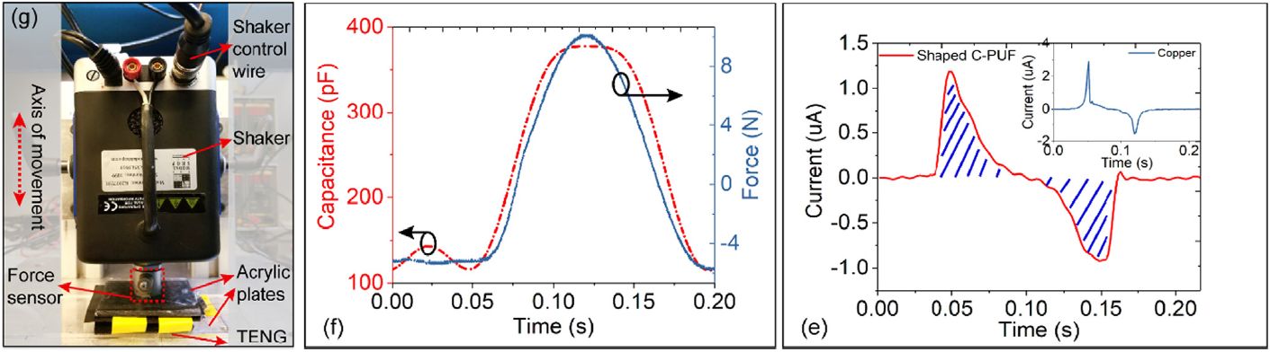
Soft TENG
We have devloped a simple flexible and progressive triboelectric nanogenerator based on macro-triangle-prism-shaped conductive polyurethane (PU) foam and polytetrafluoroethylene (PTFE) film. The proposed macro-structured conductive PU foam also integrates the functions of spring, spacer and electrode. Thanks to the innovative structures and choice of the materials, an extended current pulse width is obtained.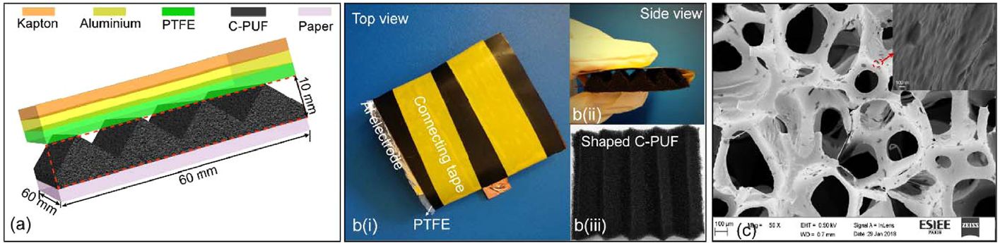
Road bump TENG
We have also proposed a road bump triboelectric generator with Bluetooth communications: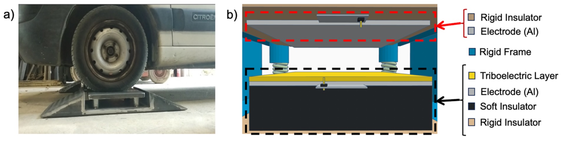

Conditioning circuit with micro-plasma switch
Rectification with stable charge pumps
We have shown that a half-wave (HW) rectifier usually performs much better than a full-wave (FW) diode bridge after a few conversion cycles. Indeed, during the early cycles, the output voltage of the FW rectifiers increases with twice the slope of the HW, although in that case both powers are far from the optimum of each circuit. However, if the output voltage of the rectifier can be set to half of its saturation voltage, HW outperforms the FW by a factor (CTENG_max/CTENG_min+1)/2.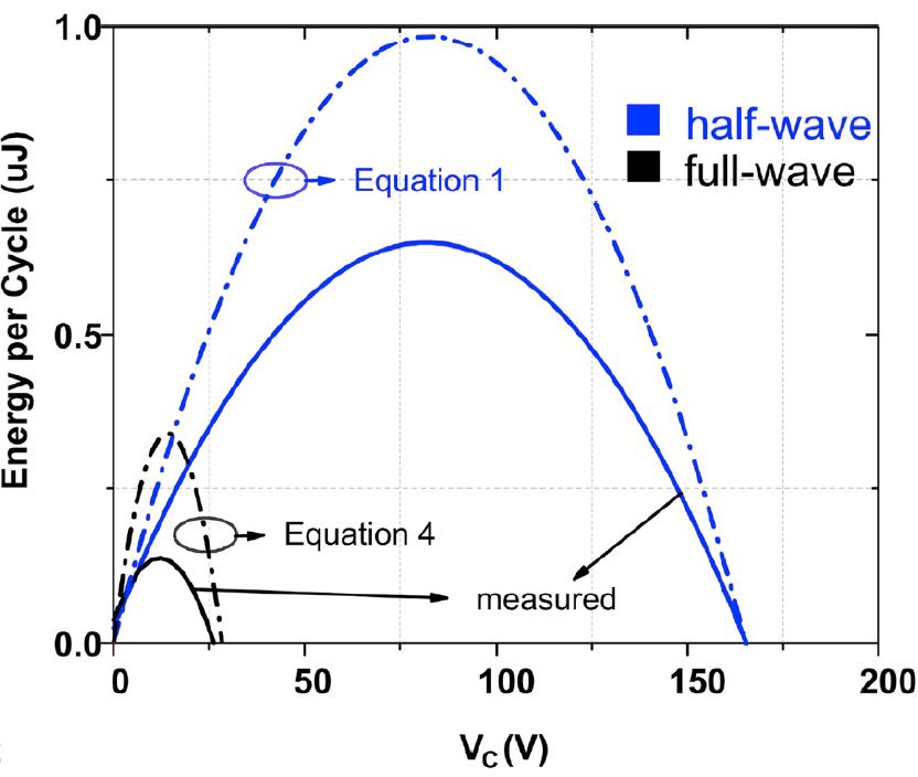
Measured and calculated energy delivered to a capacitive load as a function of VTENG for a FW and a HW diode bridge.
Rectification with unstable charge pumps
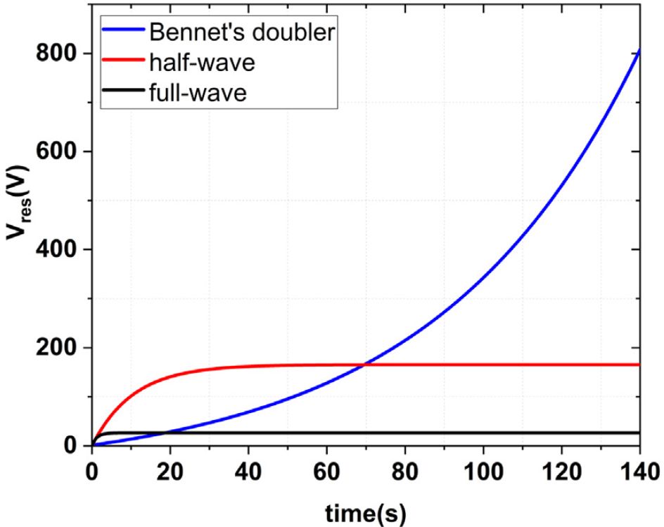
We have proposed to use the Bennet doubler with TENGs. This is a new class of conditioning circuit inspired from the electrical machines of the 18th century. It is also made of diodes and capacitors only. These circuits have the ability to exponentially increase the charge on the TENG's electrodes during operation and so to increase its bias and conversion efficiency. A minimum value of CTENG_max/CTENG_min is necessary, which is typically 2 for the most simple architecture, but it can vary depending on the circuit configuration.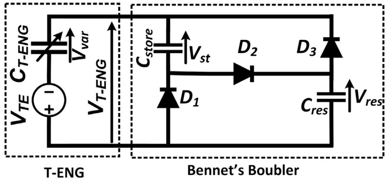
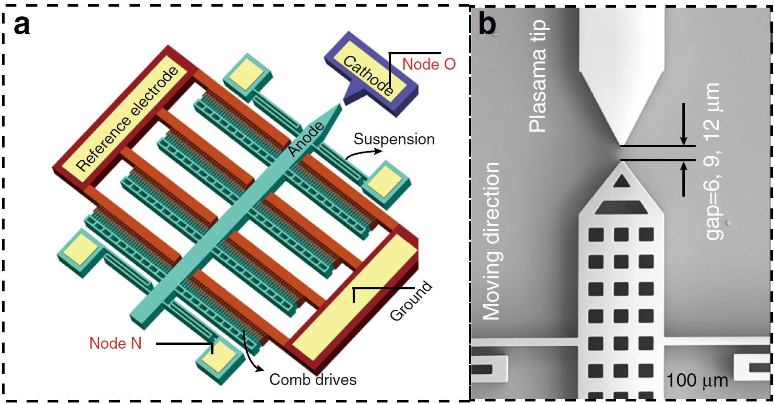
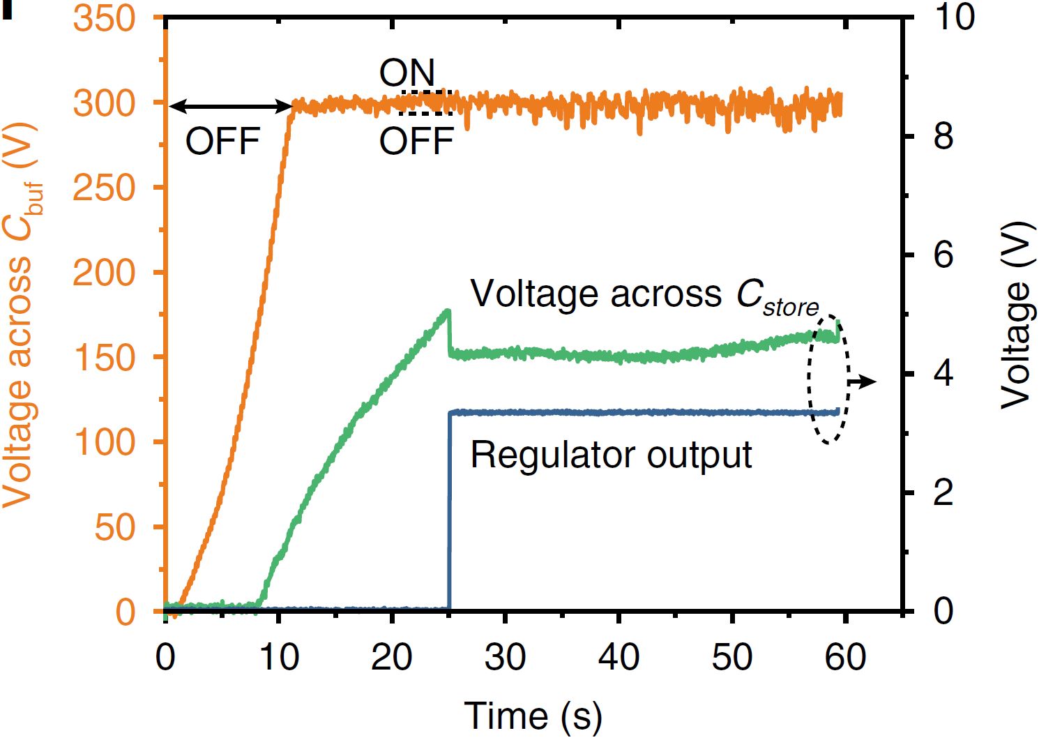
High-voltage power management using a plasma switch
Electrostatic energy harvesters need a high bias, which for TENGs is brought by an efficient triboelectric contact and/or thanks to the voltage boost from an unstable charge pumps. However, for most applications it is necessary to convert the output to a low voltage around a few volts. This can be obtained using a Buck DC-DC converter, but its switch needs to be controlled at a voltage close to the high bias value. We proposed to use a MEMS micro-plasma switch to self-control the charge transfer through a Buck circuit at high voltages. By adjusting the MEMS switch design, we can control its hysteresis in order to continuously maintain a high-bias on the transducer and hence maximize the energy conversion.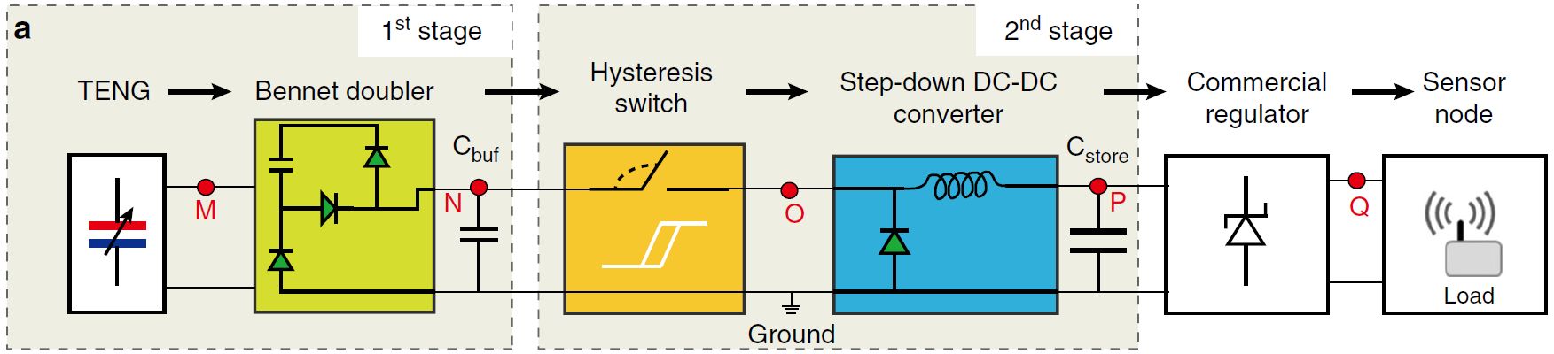
This work has been highlighted in the Electronics Insights Blog of the Electropages website.
Related publications
Modeling of TENGs
 « Road
bump triboelectric generator excited by a small number of
actuations for powering Bluetooth communications »,
A. Delbani, D. Galayko, M. Kane, et P. Basset, APL
Electronic Devices, vol. 1, no 1, p.
« Road
bump triboelectric generator excited by a small number of
actuations for powering Bluetooth communications »,
A. Delbani, D. Galayko, M. Kane, et P. Basset, APL
Electronic Devices, vol. 1, no 1, p.
-
« General
analysis and optimization of a two-stage power
management circuit for electrostatic/triboelectric
nanogenerators », H. Zhang, D. Galayko,
and P. Basset, Nano Energy, vol. 103,
p. 107816, déc. 2022, doi: 10.1016/j.nanoen.2022.107816
 “Understanding and
Modeling of Triboelectric-Electret Nanogenerator”, R.
Hinchet, A. Ghaffarinejad, Y. Lu, J. Y. Hasani, S.-W. Kim et
P. Basset, Nano Energy, vol. 47, pp. 401-409, 2018
“Understanding and
Modeling of Triboelectric-Electret Nanogenerator”, R.
Hinchet, A. Ghaffarinejad, Y. Lu, J. Y. Hasani, S.-W. Kim et
P. Basset, Nano Energy, vol. 47, pp. 401-409, 2018
- “A conditioning
circuit with exponential enhancement of output energy for
triboelectic nanogenrator”, A. Ghaffarinejad, J.
Yavand Hasani, R. Hinchet, Y. Lu, H. Zhang, A. Karami,
D. Galayko, S.-W. Kim and P. Basset, Nano Energy, vol.
51, pp. 173 – 184, 2018
Flexible TENG
- “Progressive
Contact-separate Triboelectric Nanogenerator Based on
Conductive Polyurethane Foam Regulated with a Bennet
Doubler Conditioning Circuit”, H. Zhang, Y. Lu, A.
Ghaffarinejad and P. Basset, Nano Energy, vol. 51, pp.
10-18, 2018
Conditioning circuits for TENGs and other electrostatic
kinetic harvesters
- “Employing
a MEMS plasma switch for conditioning high-voltage kinetic
energy harvesters”, H. Zhang, F. Marty, X. Xia, Y. Zi,
T. Bourouina, D. Galayko and P. Basset, Nature
Communications, vol. 11, no. 1, p. 3221, 2020
- “An Inductor-Free Output
Multiplier for Power Promotion and Management of
Triboelectric Nanogenerators toward Self-Powered Systems”,
X. Xia, H. Wang, P. Basset, Y. Zhu, Y. Zi, ACS Applied
Materials & Interfaces, Feb 5;12(5):5892-5900, 2020
- “Superior
performance of half-wave to full-wave rectifier as a power
conditioning circuit for Triboelectric nanogenerators”, A.
Ghaffarinejad, J. Y. Hasani, D. Galayko, P. Basset, Nano
Energy, Volume 66, 104137, 2019
- “A conditioning
circuit with exponential enhancement of output energy for
triboelectic nanogenrator”, A. Ghaffarinejad, J.
Yavand Hasani, R. Hinchet, Y. Lu, H. Zhang, A. Karami,
D. Galayko, S.-W. Kim and P. Basset, Nano Energy, vol.
51, pp. 173 – 184, 2018
- “Series-Parallel
Charge Pump Conditioning Circuits for Electrostatic
Kinetic Energy Harvesting”, A. Karami, D. Galayko and
P. Basset, IEEE Transactions on Circuits and Systems I:
Regular Papers, Vol. 64, no 1, pp. 227 – 240, 2016
- DOI: 10.1109/TCSI.2016.2603064
Maintained by Webmaster